Semiconductor Chiplets: Redefining the Future of Microchip Design
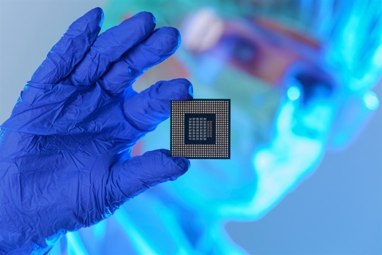
The semiconductor industry is entering a transformative era with the rise of chiplets—modular, function-specific integrated circuits that are reshaping how microchips are designed and manufactured. Unlike traditional monolithic systems-on-chip (SoCs), which integrate all functions onto a single silicon die, chiplets divide system functions into smaller, specialized blocks that work seamlessly together.
This innovative approach offers unprecedented design flexibility, cost efficiency, and scalability, helping to address the physical and economic limits of Moore’s Law. As adoption accelerates in fields like AI, data centers, and high-performance computing (HPC), chiplets are paving the way for a new generation of semiconductor technologies.
The Evolution from Monolithic SoCs to Modular Chiplets
In traditional SoC architectures, components such as CPUs, GPUs, and memory are integrated into a single die, reducing latency and power consumption. However, these designs face significant challenges, including:
- Reticle size limitations, which cap the maximum size of silicon dies.
- Decreased manufacturing yields due to larger die sizes.
- Memory bandwidth bottlenecks in data-intensive applications.
Chiplets offer a solution by separating these functions into smaller blocks that can be produced using different manufacturing processes. For instance, a CPU chiplet might be built on a cutting-edge 3nm process, while an I/O chiplet uses a more cost-effective 16nm process. This approach not only boosts performance but also reduces costs and improves manufacturing yields.
Applications and Industry Adoption
Major companies like AMD, Intel, and TSMC are leading the charge in chiplet innovation. AMD’s EPYC processors and Intel’s Ponte Vecchio GPUs showcase the immense potential of chiplets in HPC and AI workloads. The chiplet architecture allows for heterogeneous integration, enabling best-in-class combinations of components from different vendors.
By 2035, the global chiplet market is projected to reach $411 billion, driven by applications in:
- AI Accelerators: NVIDIA’s Grace Hopper Superchip combines CPU and GPU chiplets for AI-specific workloads.
- Edge Computing: Modular chiplets balance power efficiency and processing needs for IoT devices.
- 5G Infrastructure: Chiplets integrate RF, analog, and digital components for compact, low-latency communication systems.
Challenges and Future Directions
Despite their advantages, chiplets face hurdles in adoption. Standardized interconnect protocols like Universal Chiplet Interconnect Express (UCIe) are still evolving, and thermal management remains a critical challenge in densely packed systems. Additionally, a shortage of semiconductor talent threatens to slow down innovation.
Looking ahead, trends like 3D stacking and silicon photonics promise to enhance chiplet systems even further. As the industry collaborates on standards and advanced design tools, chiplets are set to become a cornerstone of next-generation computing platforms.
This shift to modularity signifies a paradigm change in how we think about semiconductors, enabling unparalleled performance, efficiency, and customization.
Read the full article on AZoNano here: Semiconductor Chiplets: The Future of Modular Microchip Design.
Sponsored by PWmat (Lonxun Quantum) – a leading developer of GPU-accelerated materials simulation software for cutting-edge quantum, energy, and semiconductor research. Learn more about our solutions at: https://www.pwmat.com/en
📘 Download our latest company brochure to explore our software features, capabilities, and success stories: PWmat PDF Brochure
📞 Phone: +86 400-618-6006
📧 Email: support@pwmat.com
Hashtags: #Semiconductor #Chiplets #MicrochipDesign #MaterialsScience #QuantumServerNetworks #PWmat


Comments
Post a Comment