Autonomous Robotic Probes: Accelerating Semiconductor Materials Discovery
Discovering new semiconductor materials that can boost the efficiency of solar cells and next-generation electronics has long been a bottlenecked process, slowed by manual testing and characterization. Now, researchers at MIT have developed an autonomous robotic probe that can rapidly measure a crucial property—photoconductance—allowing scientists to accelerate innovation in materials science.
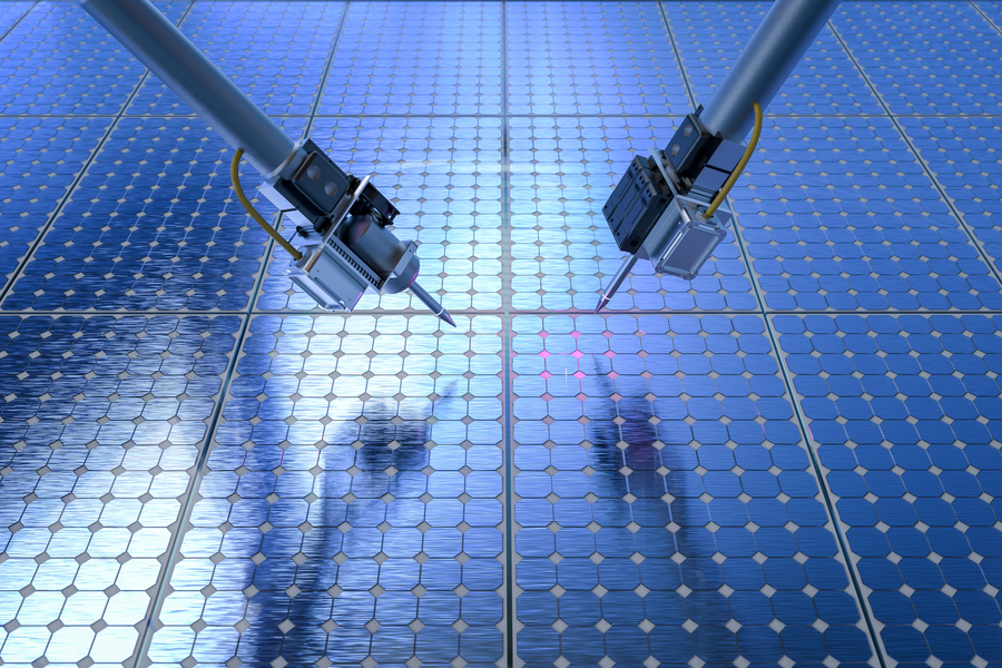
This fully autonomous system integrates robotics, machine learning, and materials science expertise to perform contact-based electrical measurements with unprecedented precision and speed. By automating the process of probing materials, the robotic system allows researchers to gather vast datasets critical for developing high-performance semiconductors, particularly for solar energy applications.
The Need for Speed in Materials Discovery
Photoconductance—how responsive a material is to light—is a key property for semiconductors used in photovoltaics and optoelectronics. Traditionally, measuring this property requires careful manual placement of probes and extensive experimentation. The MIT team’s robotic probe solves this challenge by autonomously identifying optimal contact points and executing thousands of precise measurements in a fraction of the time.
“This system opens the door for faster and more reliable discovery of semiconductor materials, with enormous implications for clean energy technologies,” explains Professor Tonio Buonassisi, senior author of the study.
How the Autonomous Probe Works
The robot begins by capturing images of perovskite samples using an onboard camera. Using advanced computer vision, it segments these images and feeds them into a neural network trained with materials science domain knowledge. This allows the system to determine the best probe contact points tailored to the shape and composition of each sample.
The robot then plans an optimal path to move between points, introducing slight randomness to improve efficiency. During a 24-hour test, the system performed over 3,000 unique photoconductance measurements—more than 125 per hour—outperforming other AI-based methods in both speed and accuracy.
The Future of Autonomous Materials Labs
As part of MIT’s vision for a fully autonomous materials discovery lab, this robotic system represents a significant leap forward. It promises to help scientists identify hotspots of high photoconductance and areas of degradation in experimental semiconductors, leading to faster breakthroughs in solar cell design and sustainable electronics.
“These robots improve the precision and repeatability of our operations, but integrating human expertise into their decision-making is key for innovation,” adds lead author Alexander Siemenn.
Read the original article here: Robotic probe quickly measures key properties of new materials.
References
Siemenn et al., “A Self-Supervised Robotic System for Autonomous Contact-Based Spatial Mapping of Semiconductor Properties.” Science Advances, July 2025.
Sponsored by PWmat (Lonxun Quantum) – a leading developer of GPU-accelerated materials simulation software for cutting-edge quantum, energy, and semiconductor research. Learn more about our solutions at: https://www.pwmat.com/en
📘 Download our latest company brochure to explore our software features, capabilities, and success stories: PWmat PDF Brochure
📞 Phone: +86 400-618-6006
📧 Email: support@pwmat.com
#Robotics #MaterialsScience #Semiconductors #AutonomousLabs #MachineLearning #QuantumServerNetworks #SolarEnergy #Innovation


Comments
Post a Comment