3D GaN-on-Silicon Hybrid Chips Could Supercharge the Future of Electronics

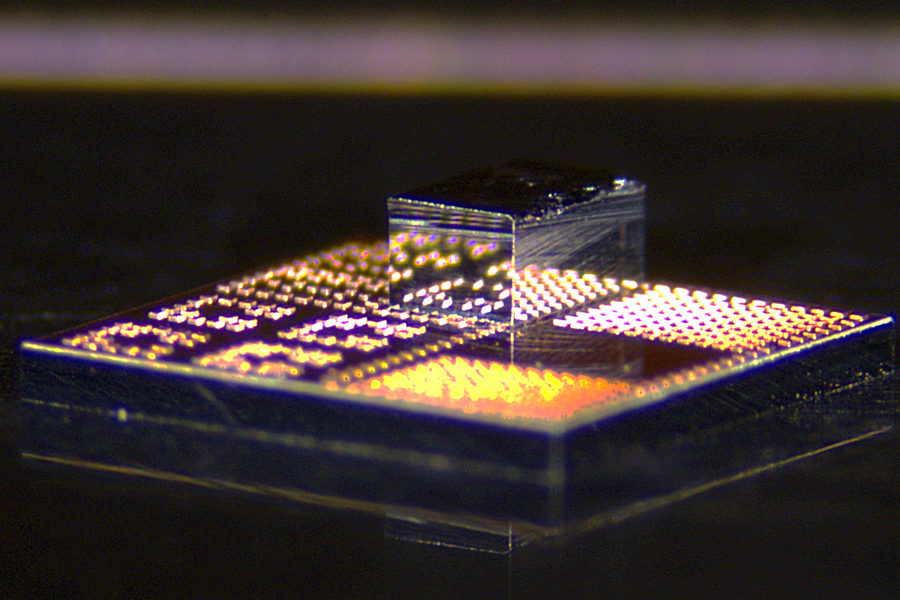
Researchers from MIT, in collaboration with the Air Force Research Laboratory and Georgia Tech, have unveiled a game-changing process that integrates high-performance gallium nitride (GaN) transistors directly onto standard silicon CMOS chips. This advancement could radically improve the speed, efficiency, and thermal management of next-generation electronics, from mobile networks to quantum computers.
Published recently and presented at the IEEE Radio Frequency Integrated Circuits Symposium, the team's method solves long-standing challenges associated with GaN’s cost and integration difficulties. The process combines the compact, high-frequency benefits of GaN with the mature infrastructure of silicon-based CMOS, without sacrificing scalability or performance.
Miniaturization Meets Power
GaN is widely regarded as the second-most important semiconductor after silicon. Its ability to operate at high voltages and frequencies makes it ideal for radar, RF circuits, power electronics, and optoelectronics. However, fabricating GaN devices is expensive, and traditional integration methods often waste large amounts of material.
The new approach involves slicing thousands of tiny GaN transistors—called dielets—from a GaN wafer and bonding only the necessary units onto a silicon chip. This not only conserves GaN but also enables superior thermal distribution and high-speed operation by scattering the GaN components across the chip's surface.
A Gold-Free, Low-Temperature Process
Traditional GaN-silicon integration often requires expensive gold bonds and high temperatures, posing contamination risks and manufacturing hurdles. The MIT team instead employed a low-cost, low-temperature copper-to-copper bonding technique that aligns perfectly with current semiconductor foundry processes.
The dielets, measuring only 240 x 410 microns, are meticulously aligned and bonded using a custom tool that operates with nanometer precision. This eliminates the need for custom GaN wafers while preserving the CMOS chip’s advanced features such as FinFETs and passive components.
Performance Boost for Power Amplifiers
To showcase the technology’s potential, the team built a 3D-millimeter-wave power amplifier using their hybrid chip. The device delivered higher gain and broader bandwidth than comparable silicon-only amplifiers—signaling tangible benefits for smartphones, 5G base stations, and edge devices requiring efficient RF transmission.
Because the process is fully compatible with existing foundry technology, it could be adopted quickly in industry—offering a pathway toward affordable, high-performance electronics and setting the stage for applications in AI hardware and cryogenic quantum systems, where GaN outperforms silicon.
Scalable, Versatile, and Ready for Tomorrow
According to MIT’s Pradyot Yadav, lead author of the study, “We’ve combined the best of what exists in silicon with the best possible gallium nitride electronics. These hybrid chips can revolutionize many commercial markets.”
As Moore’s Law slows, heterogeneous integration is becoming the key to future scaling. This project demonstrates the feasibility of combining compound semiconductors with standard CMOS, delivering more powerful, cost-effective systems that meet the rising demands of modern technology.
For more details, read the full MIT News article: https://news.mit.edu/2025/new-3d-chips-could-make-electronics-faster-and-more-energy-efficient-0618
Sponsored by PWmat (Lonxun Quantum) – a leading developer of GPU-accelerated materials simulation software for cutting-edge quantum, energy, and semiconductor research. Learn more about our solutions at: https://www.pwmat.com/en
📞 Phone: +86 400-618-6006
📧 Email: support@pwmat.com

Comments
Post a Comment